| Modified : jun. 1st. 2008 |
LOGICAL GATES
|
 |
back to summary |
 |
 |
| Description |
| Modified : jun. 1st. 2008 |
LOGICAL GATES
|
 |
back to summary |
 |
 |
| Description |
 |
 |
Schematic |
  |
|
How it works :
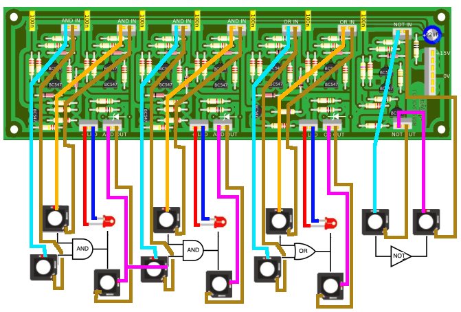
Logical AND sections: The input signals are applied to Schmitt triggers which convert these signals to proper logical levels (0V or 15V). For the first AND section, Q1-Q2 and Q4-Q5 are connected as classical discrete Schmitt triggers. R2,R3 and R7,R8 are large value resistors that insure high input impedances. Diodes D1 and D3 prevent the input transistors from negative voltages. The logical levels available at the collectors of Q2 and Q5 are applied to D2 and D4 which constitute with R12 (pull-up resistor) the actual logical AND operator. Q3 acts as a buffer and the output signal is available through R17. LD1 show the status of the output. With the values shown on the schematics the logical ON level is 10V. If a 5V level is preferred use the optional zener diode Z1 (5.1V), the PCB is provided with pads for soldering the optional zener. Logical OR section: The input signals are applied to Schmitt triggers which convert these signals to proper logical levels (0V or 15V). Transistors Q11-Q12 and Q14-Q15 are connected as classical discrete Schmitt triggers. The logical levels available at the collectors of Q12 and Q15 are applied to D10 and D12 which constitute the actual logical OR operator. Q13 acts as a buffer and the output signal is available through R47. LD3 show the status of the output. With the values shown on the schematics the logical ON level is 10V. If a 5V level is preferred use the optional zener diode Z3 (5.1V), the PCB is provided with pads for soldering the optional zener. Logical NOT section: The input signal is applied to a Schmitt trigger which converts the signal to a proper logical level (0V or 15V). Q16-Q17 are connected as a classical discrete Schmitt triggers. Q18 acts as an inverting buffer and the output signal is available through R55. |
 |
 |
Printed Circuit Board and Component Layout
|
|||
|
 |
 |
Part list and building instructions
|
||||||||||||||||||||||||||||||||||||||||||||||||||||||||||||
|
||||||||||||||||||||||||||||||||||||||||||||||||||||||||||||
| Wiring |
||||||||||||||||||||||||||||||||||||||||||||||||||||||||||||
 |
 |
 |
 |
 |
Trimming
|
| This circuit requires
no setting
or trimming. It must work right away. |
  |
  |
|
| Name :
Frédéric Monti Pseudo : zarko Modular project : Location : Gardanne, France Website : |
Name : Pseudo : sound diver Modular project : Location : UK Website : |
|
|||
 |
 |