| Modified : sep. 26th 2017 |
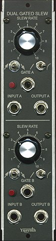
Dual GATED SLEW
|
En
français
 |
 |
back to summary |
 |
 |
| Description |
| Modified : sep. 26th 2017 |
Dual GATED SLEW
|
En
français
|
|
back to summary |
|
|
| Description |
|
|
|
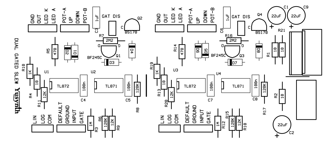
Schematic |
  |
|
The principle of this circuit is
quite simple.
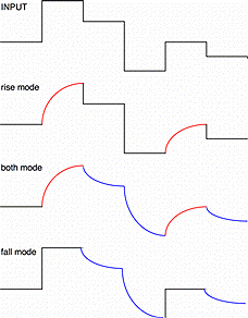
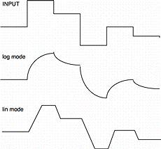
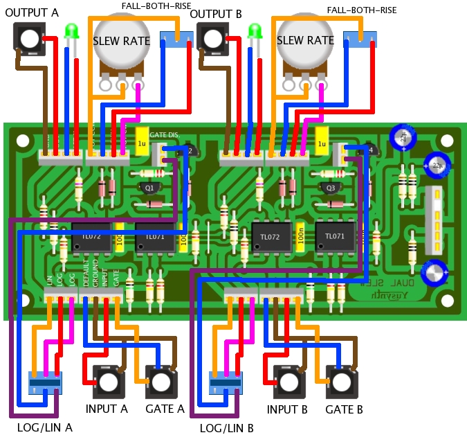
LOG mode : In the LOG mode, U1a acts as a simple voltage follower (pin 6 is fedback to pin 2), it buffers the input signal. Let's consider that SW1 is in it's middle position, in such a case the voltage at the output of U1a (pin 6) is going to either charge C3 (if this voltage is higher than that at C3) or dischage C3 (if this voltage is lower than that at C3) through R4 and P1. The greater the value of P1, the longest the charging/discharging time. Then U1b acts as a simple voltage follower and buffers the voltage at C3 to the output. If we toggle SW1 on the Up lug, then diode D2 bypasses the SLEW RATE potentiometer P1, in such a case the discharging rate of C3 will only depends on R4 (10 ohms) and thus is very fast, while the charging rate still depends on P1. Now if we toggle SW1 on the Down lug, now it's diode D1 that bypasses P1 and therefore it's the charging rate of C3 that becomes very fast and the discharging rate still depends on P1. GATED mode : Now let's consider the part played by the FET transistor Q1, in this configuration it acts as a bypass switch for P1 when a positive voltage is applied to the grid of Q1 (the drain-source resistance drops to 50 to 60 ohms). When a negative voltage (which is the default) is applied to the grid of Q1, the drain-source resistance rises to few megohms and P1 becomes active. When no jack is plugged in the GATE input, R11 is connected to the input of the comparator built with U2, this positive voltage is higher than the reference voltage set by the the voltage divider made with R8 and R9. Therefore the output of U1 is negative and opens the FET switch Q1. At the same time this voltage sets the grid of Q2 to 0V (D4 blocks the negative voltage), the drain-source resistance of Q2 is nearly infinite and the current circulating through R10 feeds LD1 which in turns emit a RED light. If a jack is connected to the GATE input and the GATE voltage is 0V, the comparator switches and a positive voltage appears on its output. This positive voltage makes Q1 and Q2 conductive that is their drain-source resistance becomes negligible. As consequence P1 and LD1 are bypassed, the SLEW rate becomes very fast (few ms) and the LED is dark. If a positive (>1.5V) voltage is applied at the GATE input, the comparator toggles and a negative voltage is applied to the grids of Q1 and Q2, P1 becomes active and the LED brightens. LIN mode : In this mode U1 is no longer a voltage follower of the input voltage but is also controlled by the output voltage of the modules (output of U1b is fed back to the inverting input of U1b). In such a configuration the charging/discharging current of C3 is no longer depending on the instantaneous charge of C3 but is maintained constant. Because this current remains constant the charging/discharging curve of C3 remains linear. However in this feedback loop the Q1 FET transistor will no longer behave as simple switch, that's why in the linear mode the switch SW2-2 disconnects Q1. |
|
|
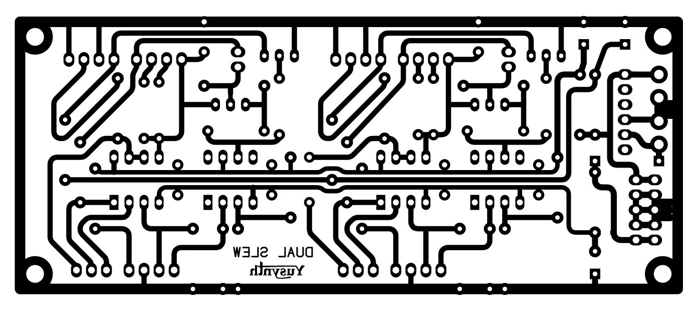
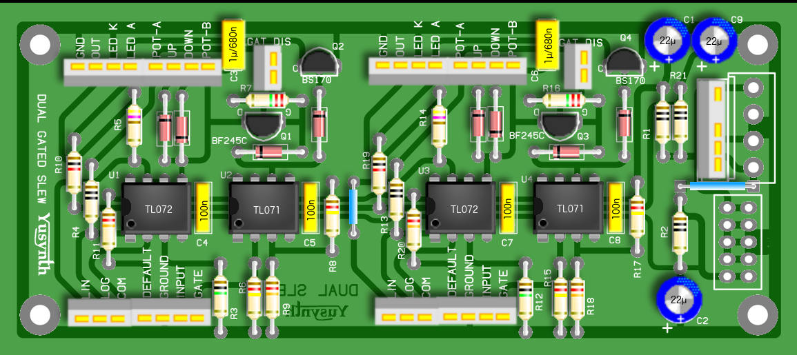
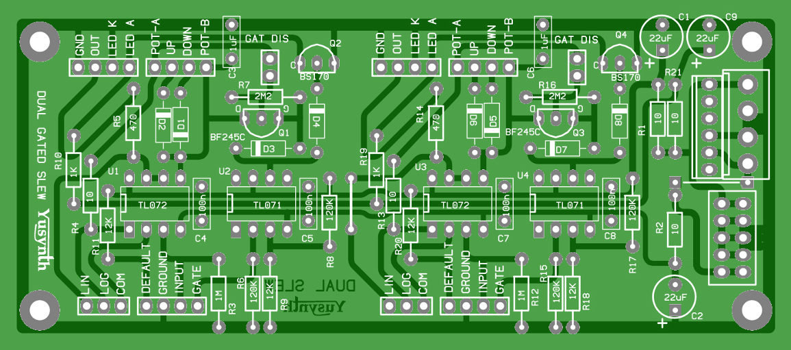
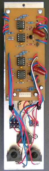
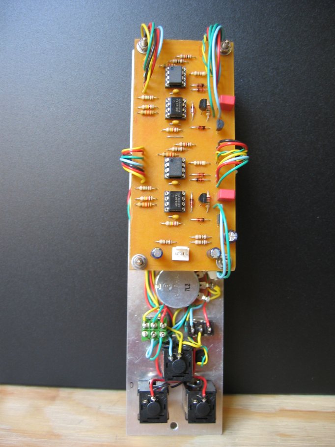
Printed Circuit Board and Component Layout
|
|||
|
|
|
List of parts and building instructions
|
|||||||||||||||||||||||||||||||||||||||||||||||||||||||||||||||
|
|||||||||||||||||||||||||||||||||||||||||||||||||||||||||||||||
| Wiring |
|||||||||||||||||||||||||||||||||||||||||||||||||||||||||||||||
 |
|
|
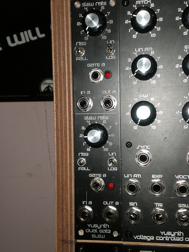
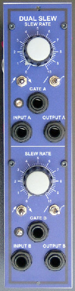
| Front plate |
||
|
|
|
Trimming
|
| This circuit requires
no setting
or trimming. It must work right away. |
|
|
References |
Information and
datasheet for BF245  Information and datasheet for BS170 |
 |
 |
  |
| Name :
Patrick Pseudo : Baronrouge Modular project: JHC live lab Location: Toulon, France Web site : http://myspace.com/patjhc |
Name : Pseudo : Julien Modular project: Location : France Web site : |
Name : Pseudo : Sebo Modular project : Location : Argentina Website : http://www.cosaquitosenglobo.com.ar |
  |
||
| Name : Zarko Modular project : Location : Gardanne, France Website : |
|
|||
|
|