| Modified : mar. 12th 2009 |
Dual PULSE DELAY
|
En
français
 |
 |
back to summary |
 |
 |
| Description |
| Modified : mar. 12th 2009 |
Dual PULSE DELAY
|
En
français
|
|
back to summary |
|
|
| Description |
|
|
|
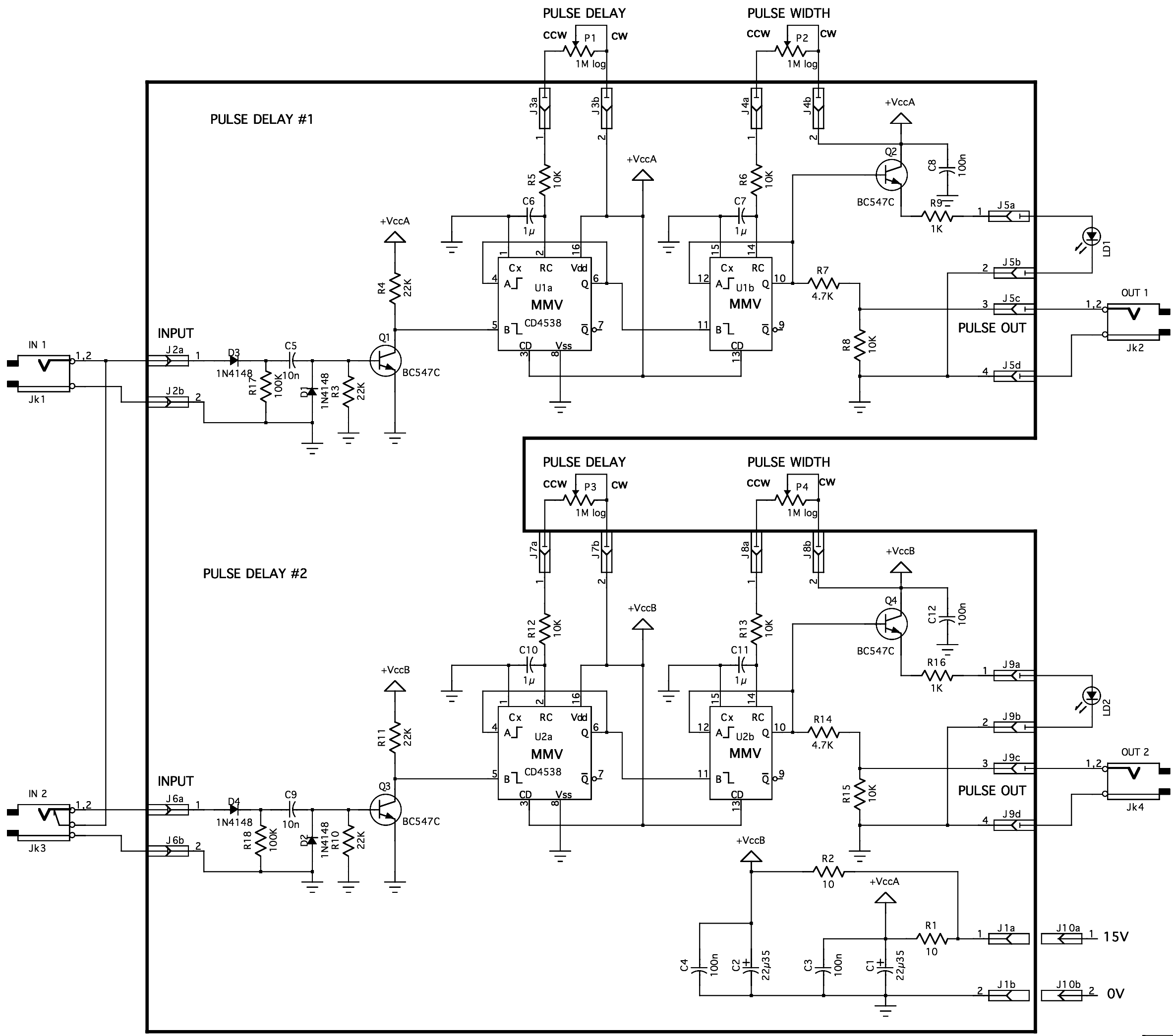
Schematic |
 |
|
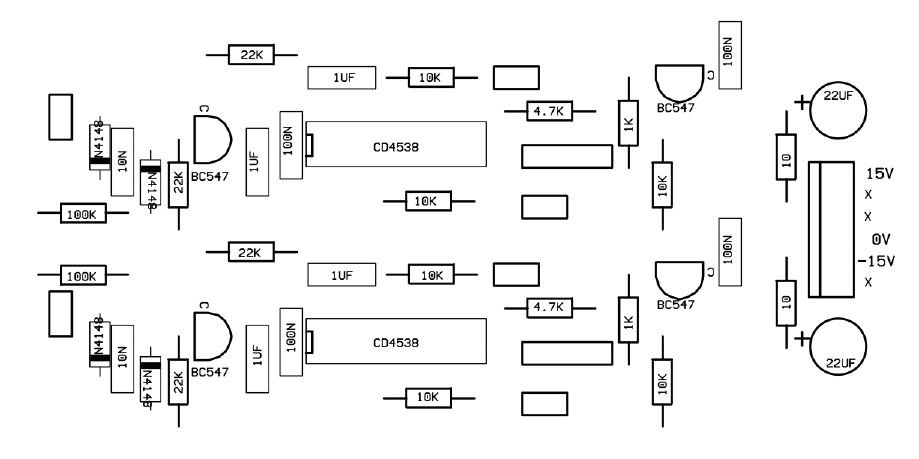
The principle of this circuit is
quite simple and rely on the use of a dual monostable CD4538 IC.
Here is how it operates : when a GATE signal (between 3V and 15V), the capacitor C5 acts as a differenciator and converts the gate signal into a brief positive pulse (width 10 ms). D1 protects the circuit from negative voltages. The brief pulse created on the rising edge of the GATE signal make Q1 briefly conductive and the voltage at its collector falls down to 0.2V. The collector is connected to the falling edge trigger pin of U1a. This triggers the monostable U1a and its output Q goes to a high level and stays there for a duration set by the RC cell built around (R5+P1)C6, P1 is a 1M log potentiometer and the delay can be set between 1ms and 1s. After this delay Q returns to the low level and in turn triggers the second monostable U1b whose output Q goes to the high level and stays there for a duration set by the RC cell built around (R6+P2)C7, P2 is a 1M log potentiometer and the delay can be set between 1ms and 1s. The output Q is connected to a voltage divider (R7,R8) that delivers the OUTPUT PULSE with a amplitude of 10V. The base of Q2 is connected to the Q output of U1b and drives the LD1 LED. |
|
|
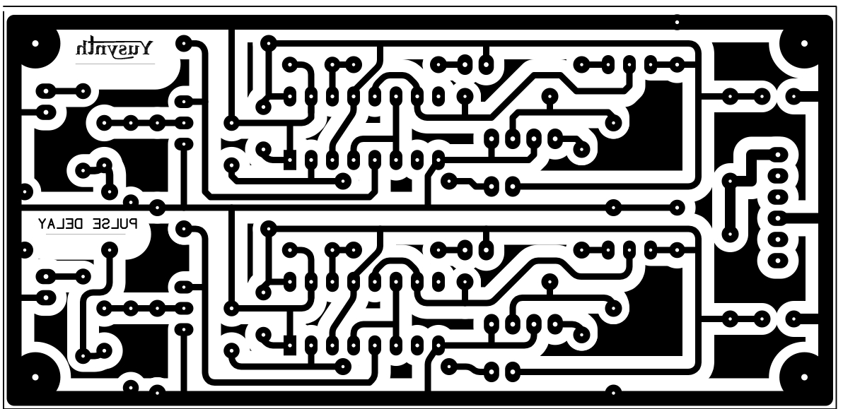
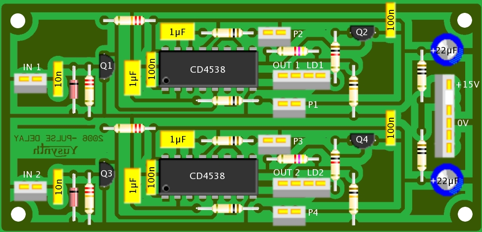
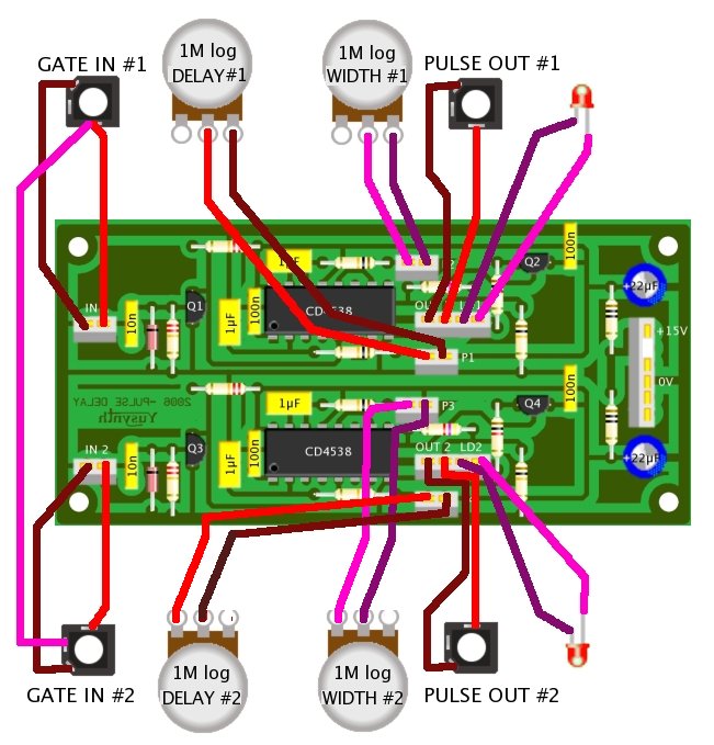
Printed Circuit Board and Component Layout
|
|||
|
|
|
List of parts and building instructions
|
|||||||||||||||||||||||||||||||||||||||||||||||||||
|
|||||||||||||||||||||||||||||||||||||||||||||||||||
| Wiring |
|||||||||||||||||||||||||||||||||||||||||||||||||||
 |
|
|
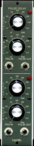
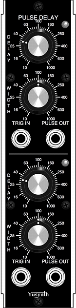
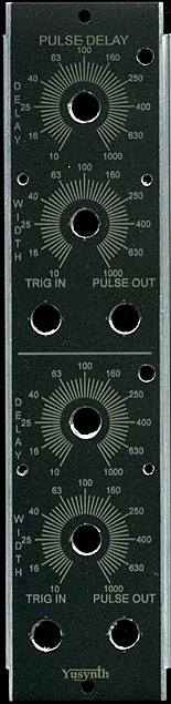
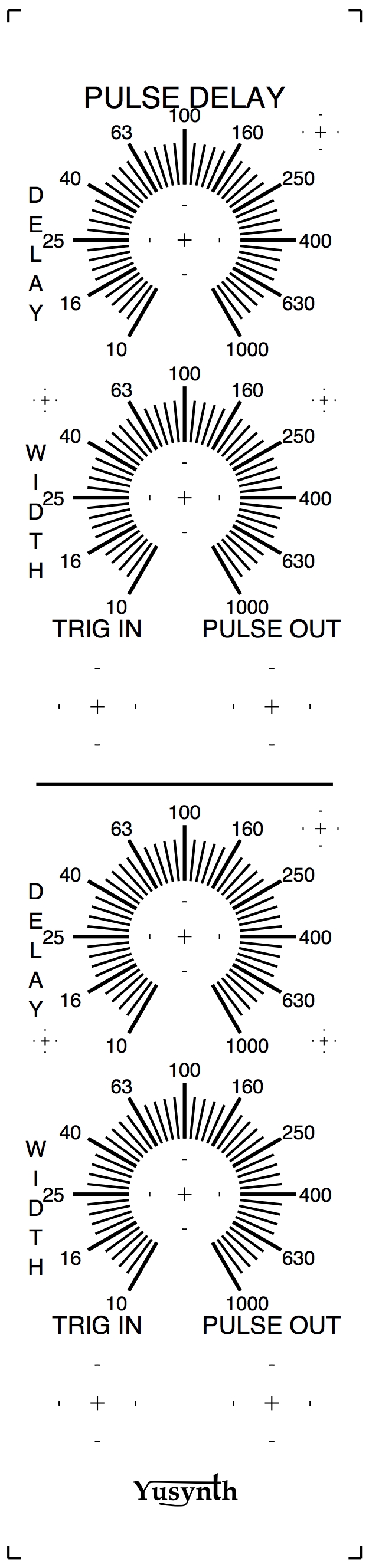
| Front plate |
|||
|
|
|
Trimming
|
| This circuit requires no setting
or trimming. It must work right away. |
|
|
References |
Information and datasheet for
CD4538  Information and datasheet for BC547 |
 |
|
|
| Name
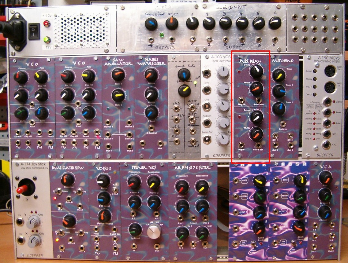
: Patrick Pseudo : Baronrouge Modular project: JHC live lab Location Toulon, France Web site : http://myspace.com/patjhc |
|
|
|||
|
|