| Update nov. 25th, 2016 |
Noise generatorSample & Hold
|
En français
 |
 |
back to summary |
 |
 |
| Description |
| Update nov. 25th, 2016 |
Noise generatorSample & Hold
|
En français
|
|
back to summary |
|
|
| Description |
|
|
|
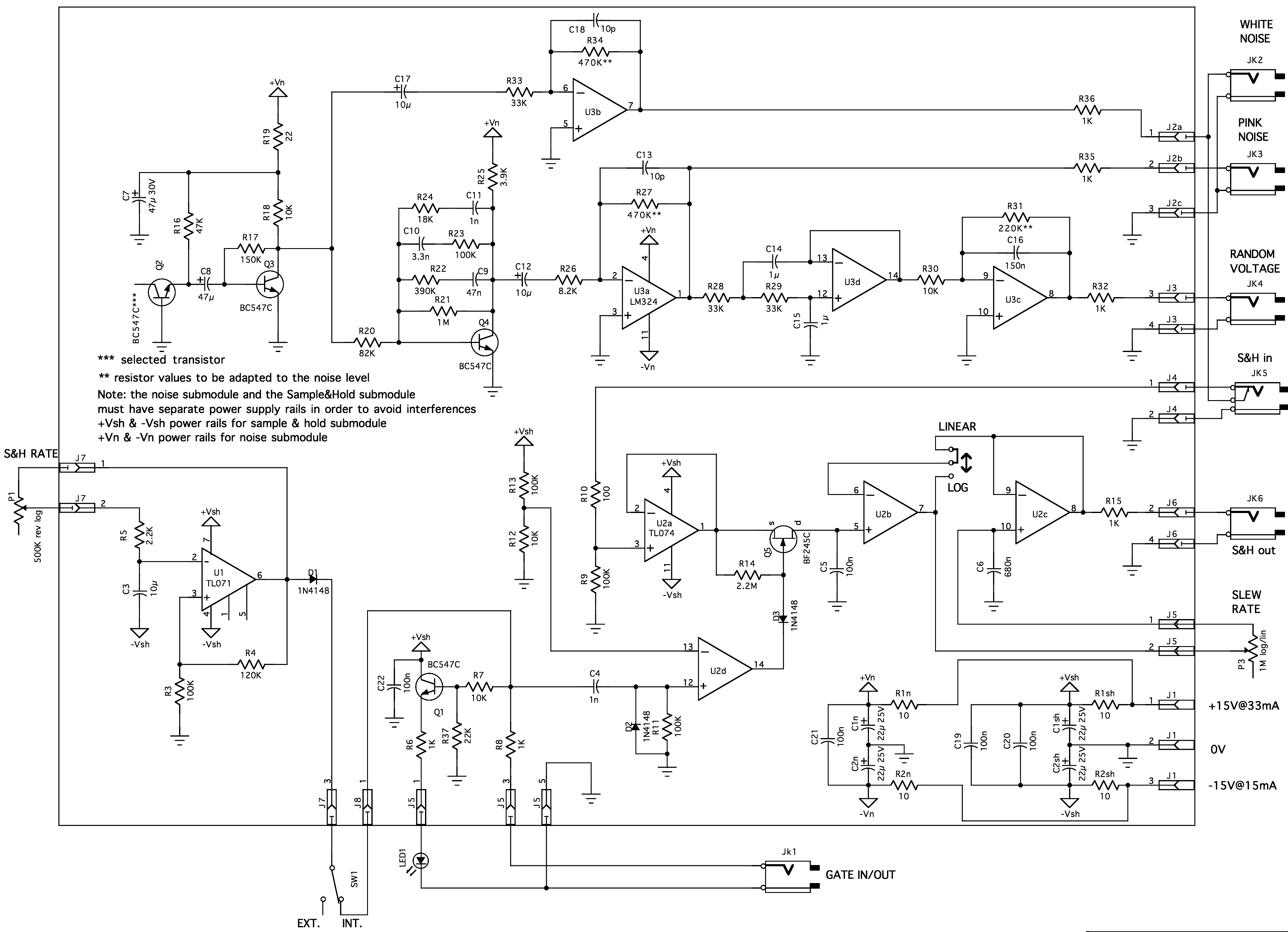
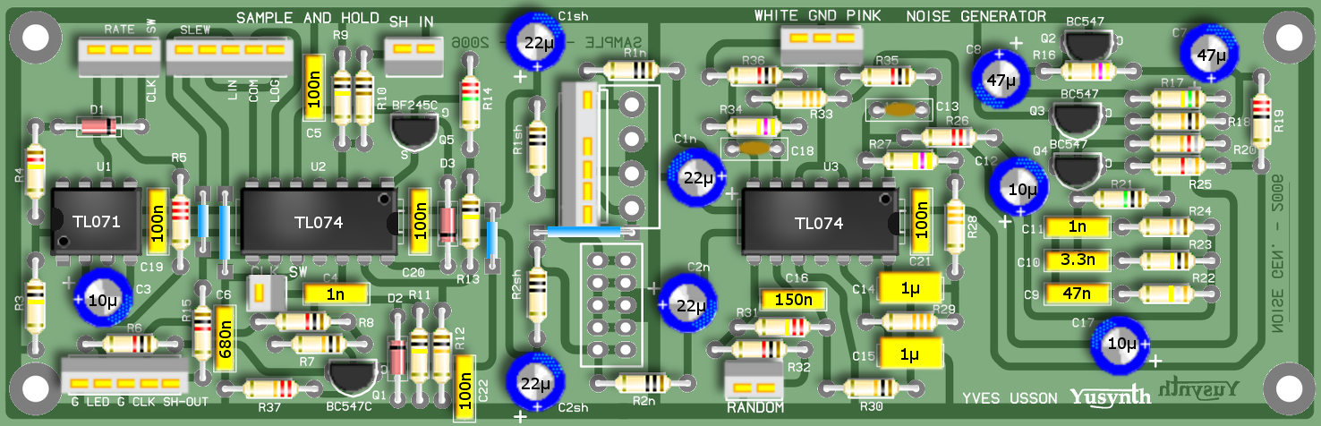
Schematics |
 |
|
Separate supply rails are used for
the two sub-modules. This was made necessary to solve an
issue on
my first prototype, the clock and trigger stages of the S&H
were interfering with the noise amplifier stage of the
noise generator!
Noise submodule : Q2 is connected
as a reverse polarised diode in order to generate as
much noise as possible. This noisy signal is first
amplified by Q3 and routed both to U3b which amplifies
the white noise signal and to Q4. A network or
resistor-capacitors (R2-R24,C9-C11) shapes the
spectrum. The result is a low-pass filtering with a
3dB/octave slope giving rise to the so-called pink
noise. Then the pink noise is amplified by U3d
which is followed by two low-pass filters to provide
slow varying random voltages. The first filtering
stage is second order low-pass with a cut-off
frequency close to 5Hz the second stage provides a
6dB/octave lowpass with a cut-off frequency of 4.7Hz
with some amplification in order to level up the
random voltage.
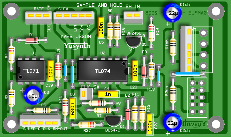
Sample and Hold : U1 is an OPA in a classical astable multivibrator configuration, with the values of R3, R4, R5, C3 and P1 the slowest rate is 0.1Hz and fastest 10Hz. The positive part of the pulse is selected by D1 and routed to a switch that is used to toggle the S&H trigger between the internal clock and an external clock. Q1 drives a LED which flashes as a function of the clock rate. C4 differentiates the clock signal in order to convert the rising edge of the clock into a brief positive pulse (10ms). U2d is connected as a comparator. D2 selects the negative part of the pulse to drive the gate of the Q2 FET. |
|
|
|
|
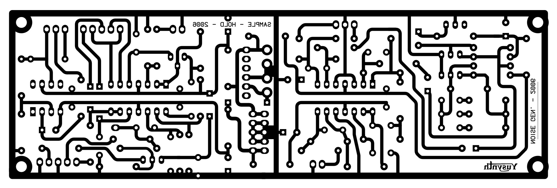
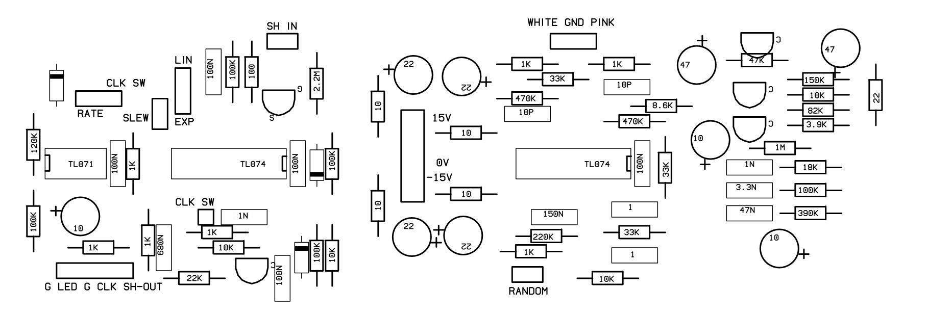
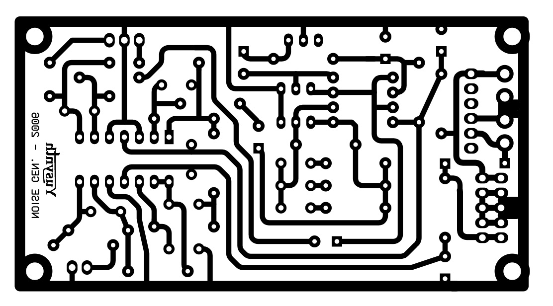
Components and building details |
|||||||||||||||||||||||||||||||||||||||||||||||||||||||||||||||||||||||||||||||||||||||
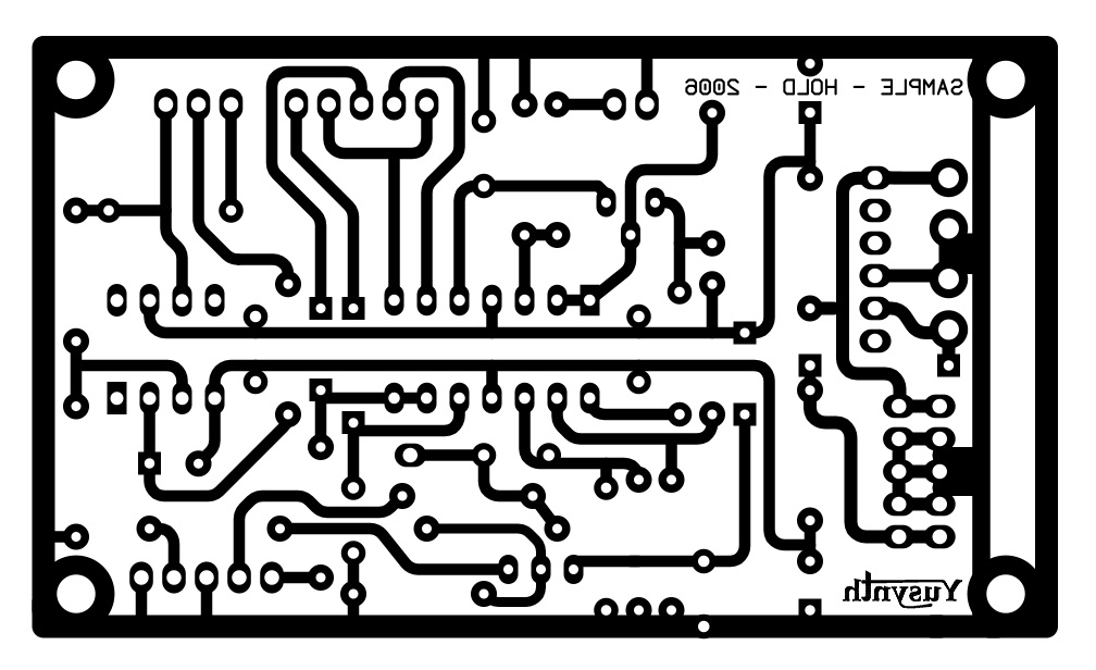
| Sample and Hold submodule |
|||||||||||||||||||||||||||||||||||||||||||||||||||||||||||||||||||||||||||||||||||||||
|
|||||||||||||||||||||||||||||||||||||||||||||||||||||||||||||||||||||||||||||||||||||||
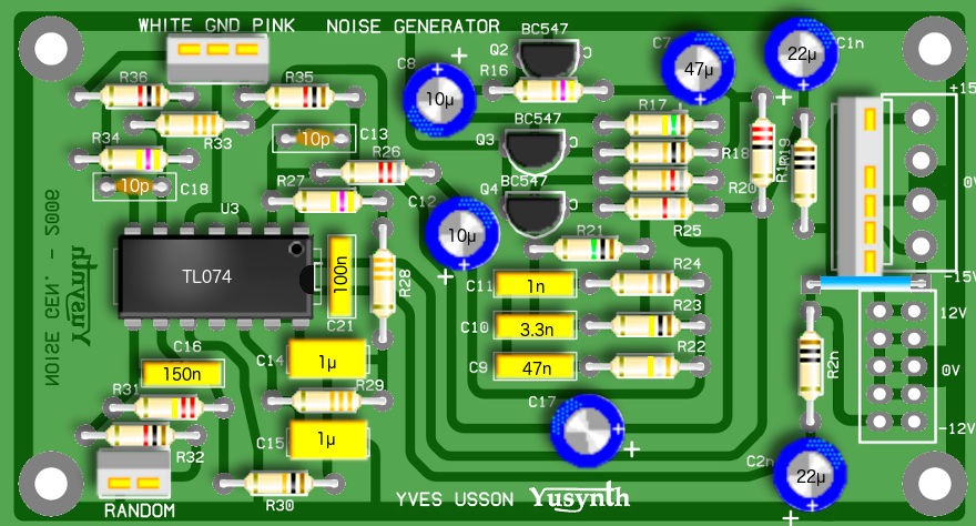
| Noise generator sub-module | |||||||||||||||||||||||||||||||||||||||||||||||||||||||||||||||||||||||||||||||||||||||
|
|||||||||||||||||||||||||||||||||||||||||||||||||||||||||||||||||||||||||||||||||||||||
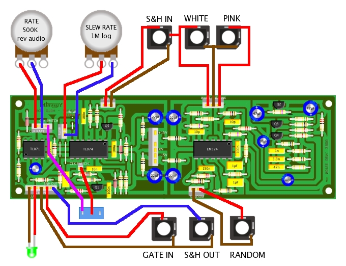
| Wiring |
|||||||||||||||||||||||||||||||||||||||||||||||||||||||||||||||||||||||||||||||||||||||
 |
|
|
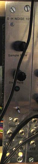
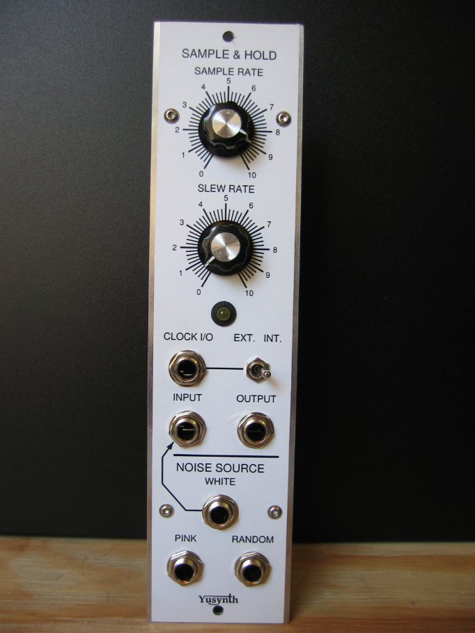
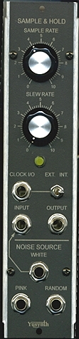
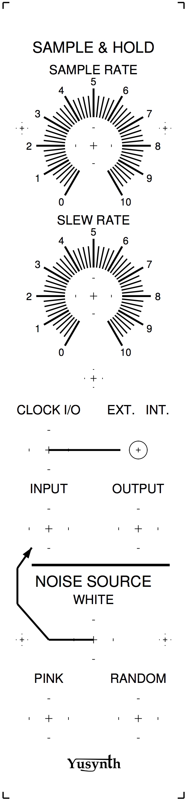
| Front panel |
||
|
|
|
Setting and trimming
|
|
The trimming is
quite simple, it consists of taking a batch of BC547
transistors and selecting among these which one
gives the highest white noise level while being
symetrically balanced around 0V level, with the
flatest spectrum. In order to do so, it is a good
idea to use a transistor socket for Q2, this way one
can swap easily the transistors to find the best
one. It is a good practice to wait about 1min before
checking the noise level and quality of white
spectrum in order that Q2 has reached a steady
temperature.
Below are the spectra I measured on the two boards I built. Some resistor values may also be adjusted to obtain the desired output levels. 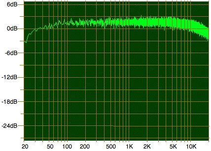 Measured audio spectrum - white noise output (0dB position set arbitrarily) 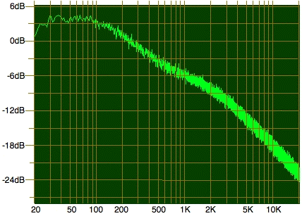 Measured audio spectrum - pink noise output (0dB position set arbitrarily) |
|
|
References |
| Here are some
interesting references concerning noise generation
and noise properties : Grant Richter's spectral and probability distributions :  Eliott sound project : |
 |
 |
  |
| Name : Czaba
ZVEKAN Modular project : Location : Basel, Switzerland Website : |
Name
: Patrick Pseudo : Baronrouge Modular project: JHC live lab Location Toulon, France Web site : http://myspace.com/patjhc |
Name :
Federic Monti
Pseudo : Zarko Modular project: Location Gardanne, France Web site : |
|
|||
|
|


