| Modified : dec. 13th. 2008 |
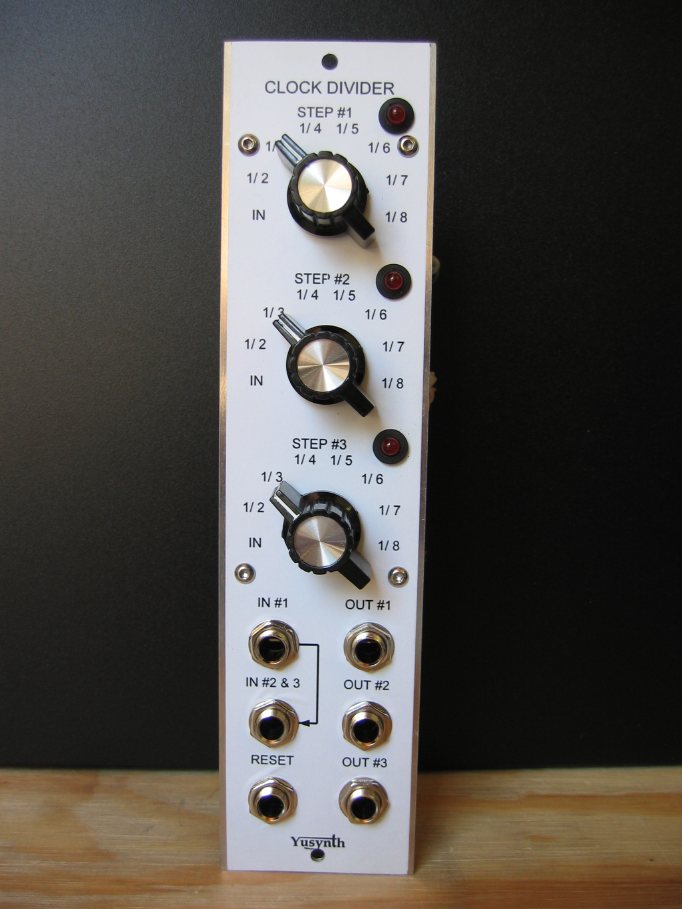
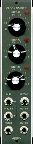
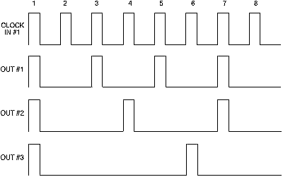
CLOCK DIVIDER
|
En
français
 |
 |
back to summary |
 |
 |
| Description |
| Modified : dec. 13th. 2008 |
CLOCK DIVIDER
|
En
français
|
|
back to summary |
|
|
| Description |
|
|
|
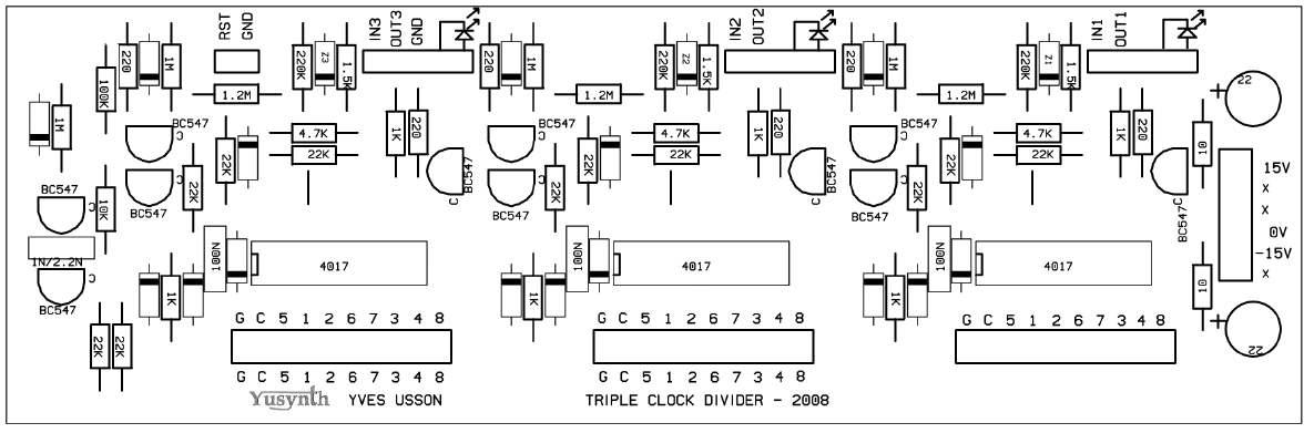
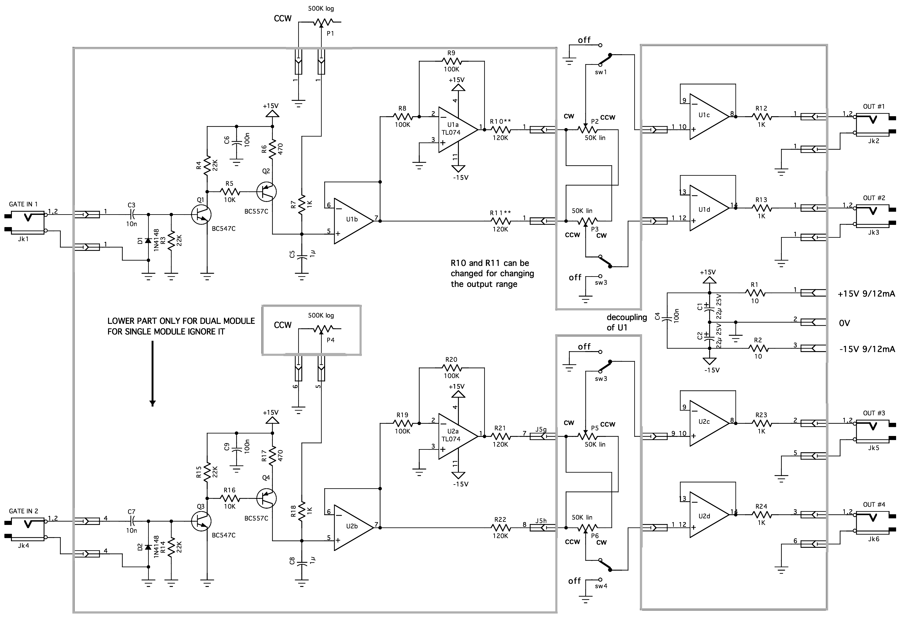
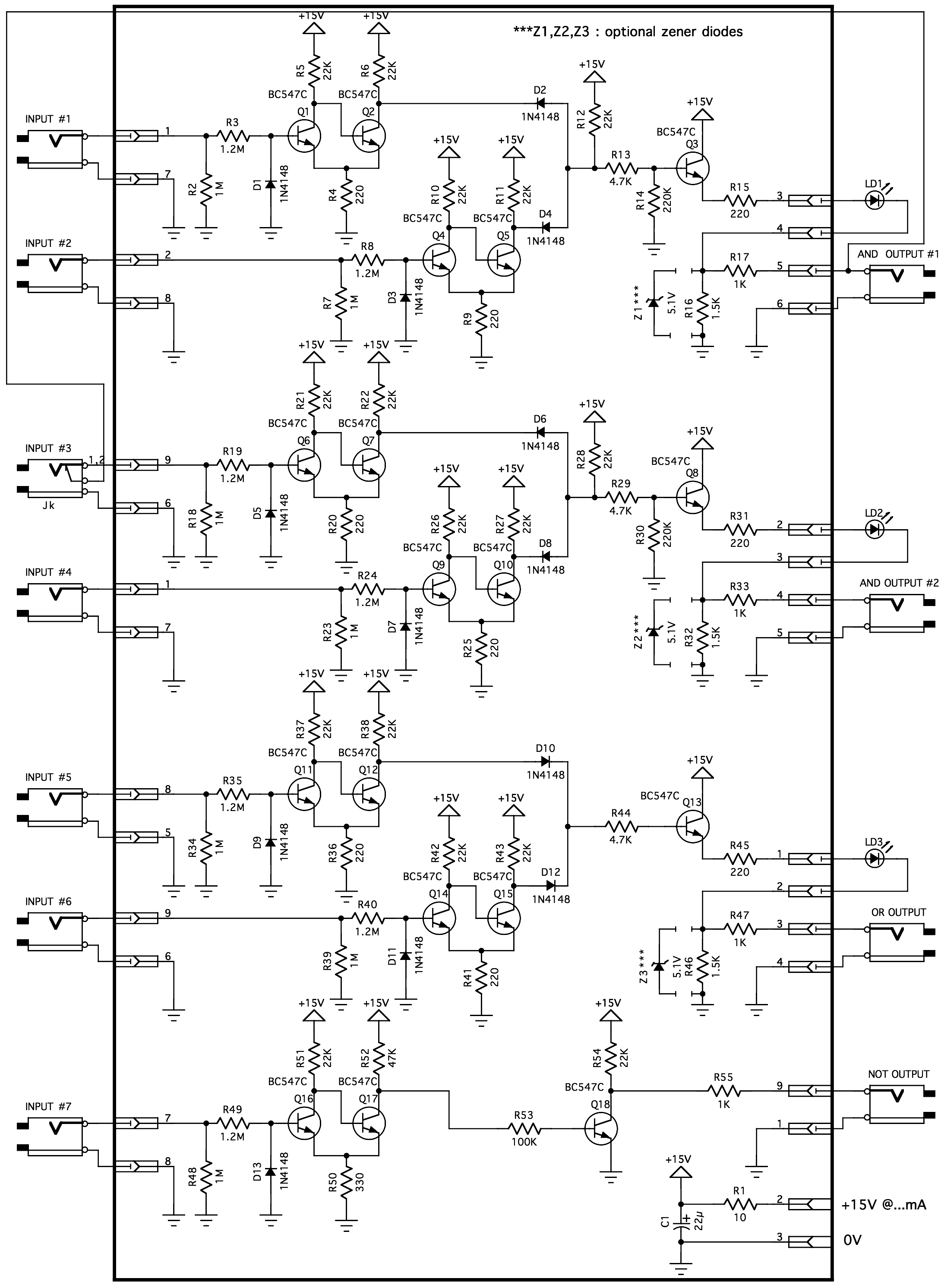
Schematic |
|
|
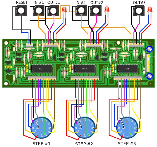
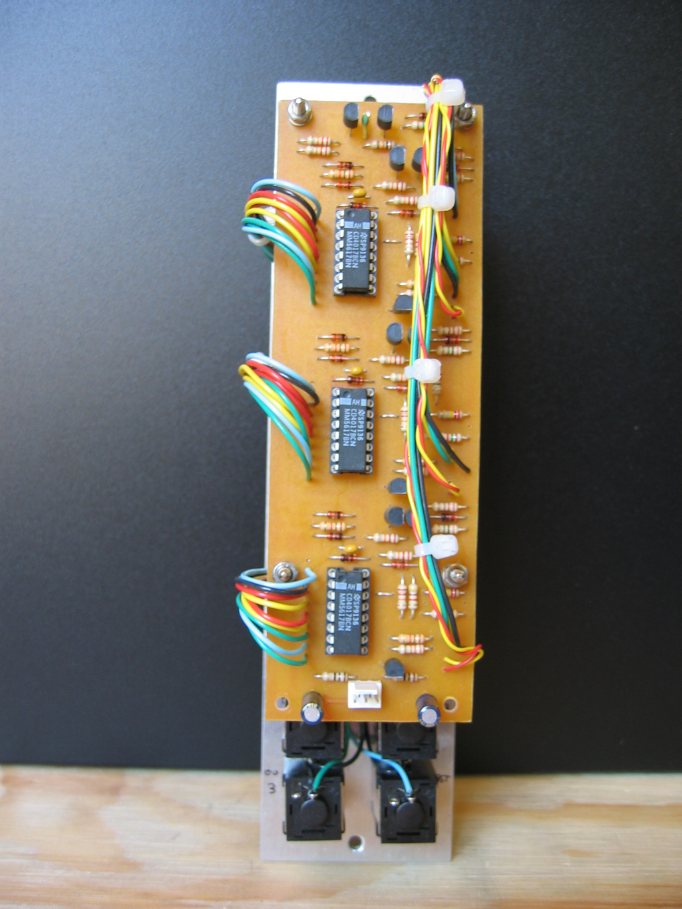
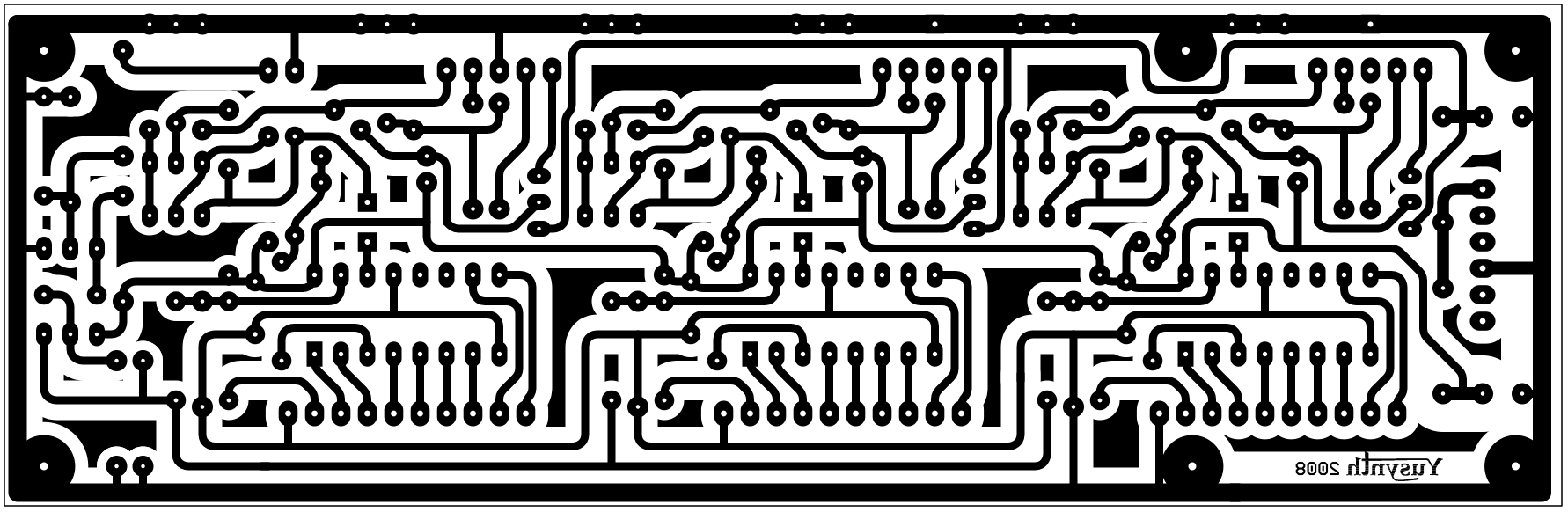
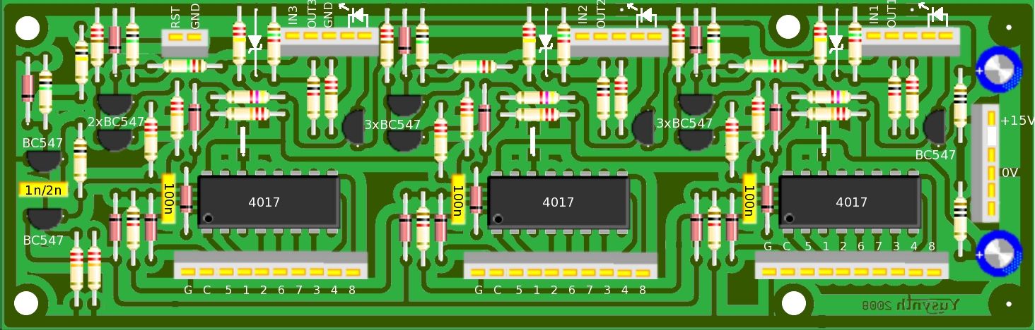
Printed Circuit Board and Component Layout
|
|||
|
|
|
Part list and building instructions
|
|||||||||||||||||||||||||||||||||||||||||||||||||||||||||||||||
|
|||||||||||||||||||||||||||||||||||||||||||||||||||||||||||||||
| Wiring |
|||||||||||||||||||||||||||||||||||||||||||||||||||||||||||||||
 |
|
|
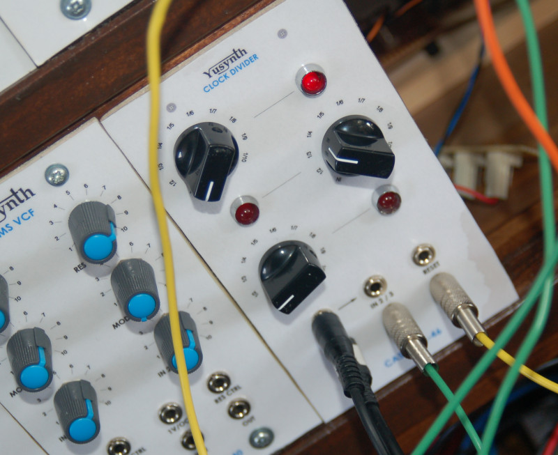
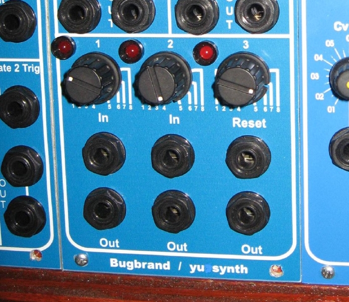
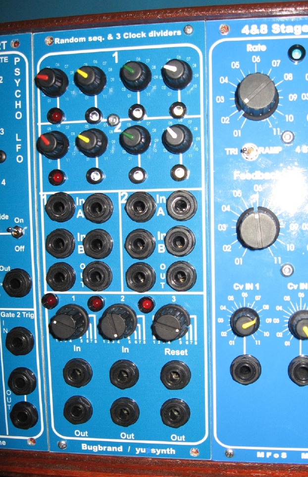
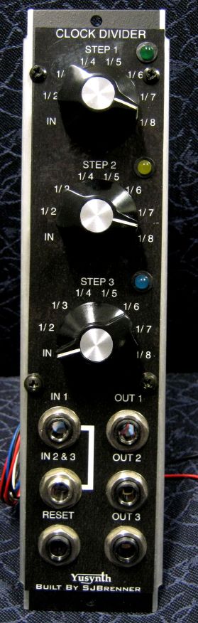
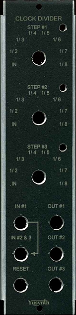
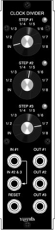
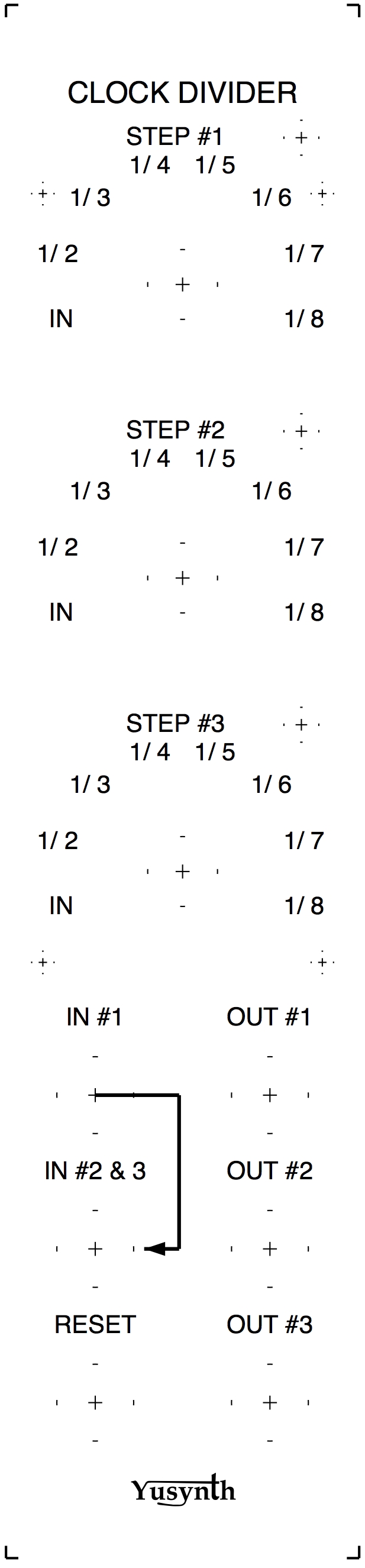
| Front plate |
||
|
|
|
Trimming
|
| This circuit requires no setting
or trimming. It must work right away. |
 |
  |
  |
| Name
: Pseudo : Etaoin Modular project : Casia MS01 Location : Utrecht, Netherlands Website : www.casia.org/modular |
Name
: David Wood Pseudo : Skrog Modular project : Skrog Productions Location : Galashiels , Scotland Website : www.myspace.com/skrogproductions |
Name
: Frédéric Monti
Pseudo : Zarko Modular project : Location : Gardanne, France Website : |
  |
||
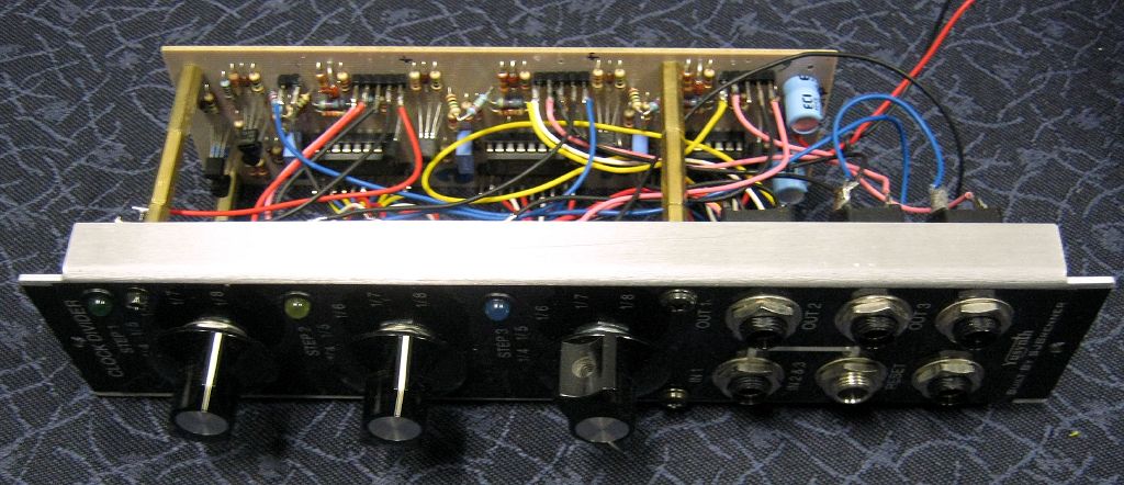
| Name
: Steven Brenner Pseudo : Modular project : Location : Waterloo, Ontario, Canada Website : |
|
|||
|
|


