| Update : may 8th, 2017 |
Mini-Maxi Voltage Processor |
En français
 |
 |
back to summary |
 |
 |
| Description |
| Update : may 8th, 2017 |
Mini-Maxi Voltage Processor |
En français
|
|
back to summary |
|
|
| Description |
|
|
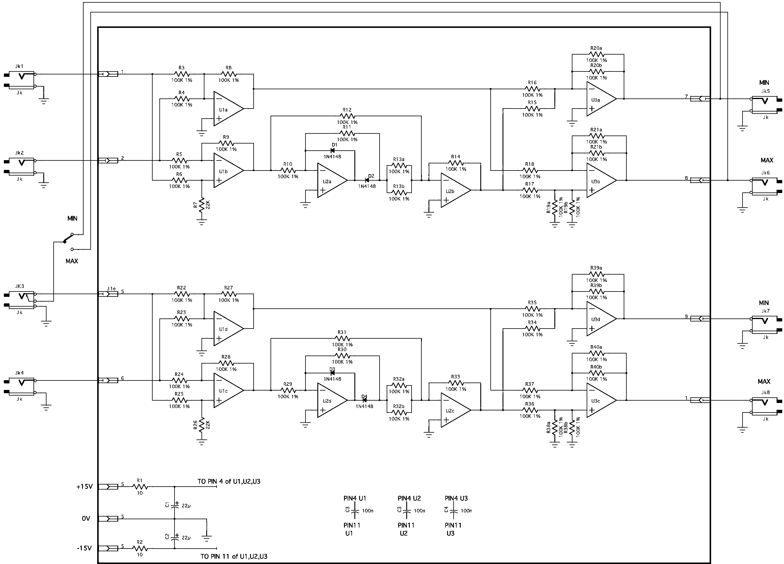
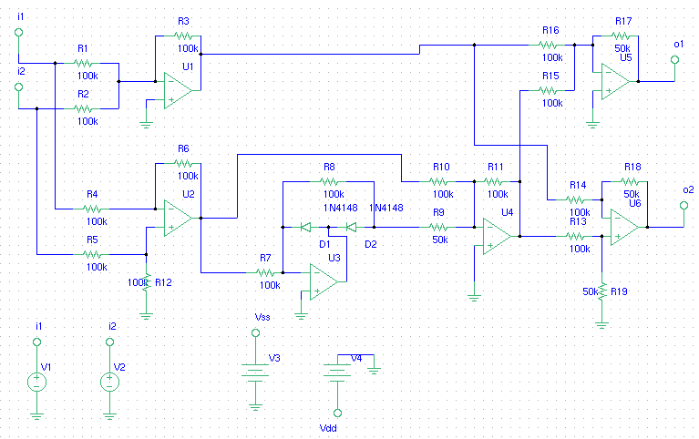
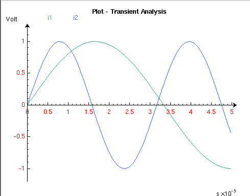
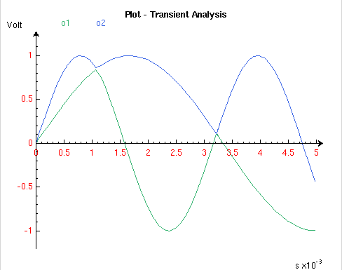
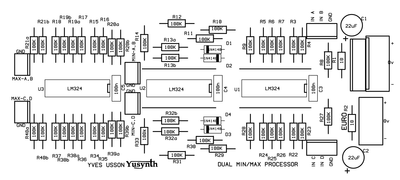
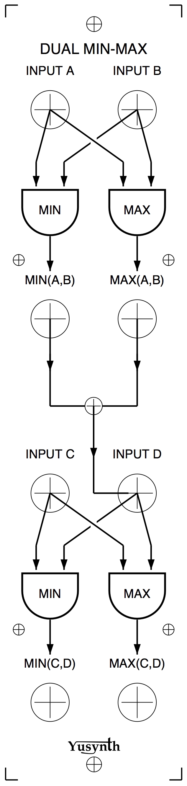
Schematic diagram
|
 |
|
|
|
|
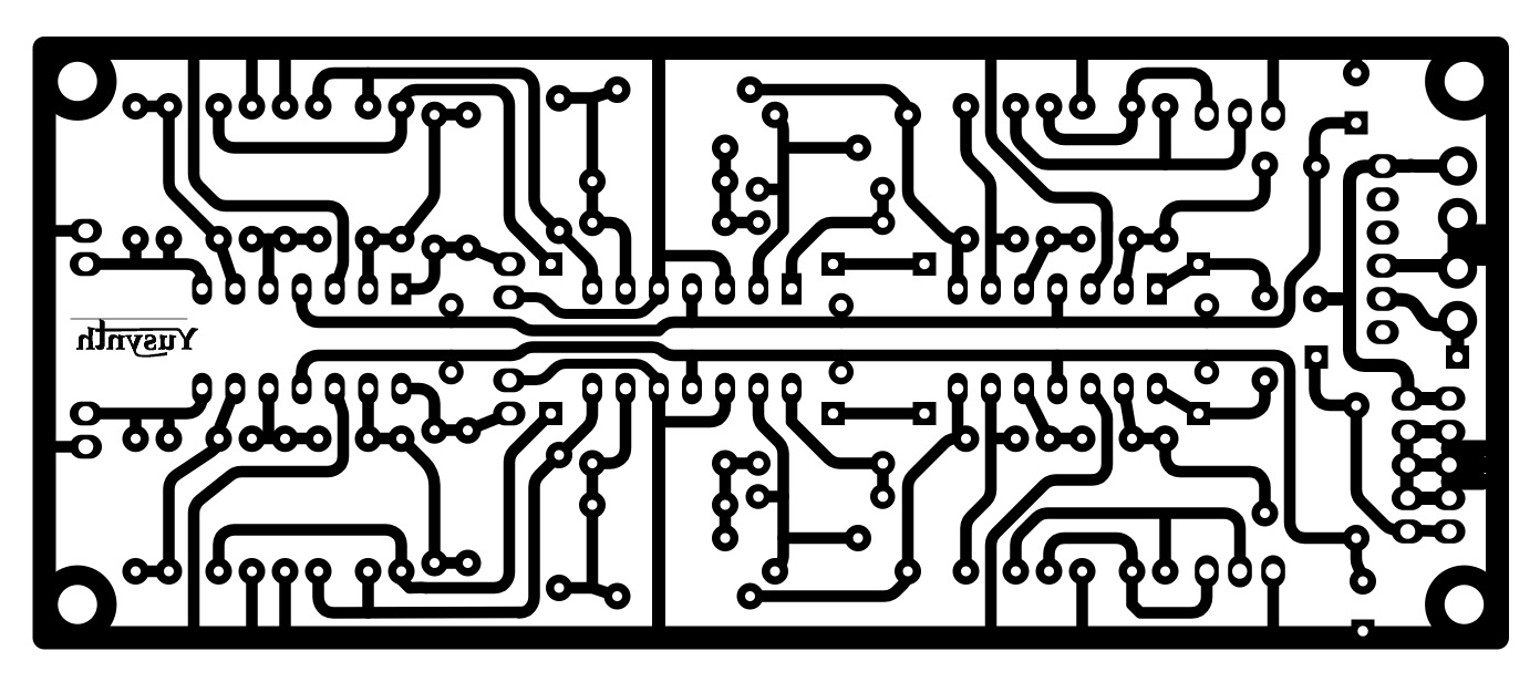
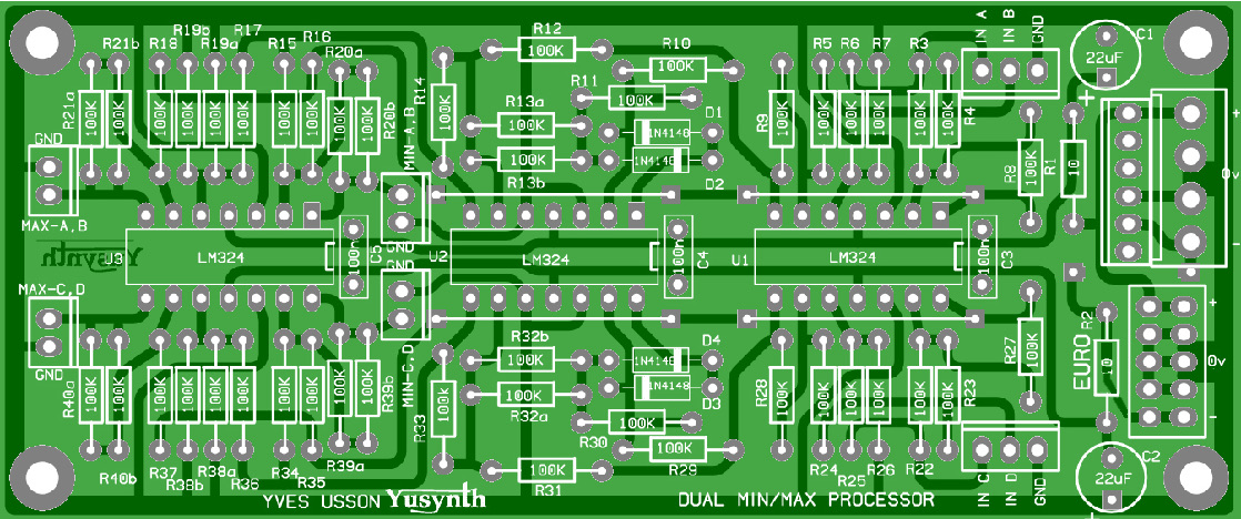
Building instructions
|
|||||||||||||||||||||||||||
|
|||||||||||||||||||||||||||
| |
|||||||||||||||||||||||||||
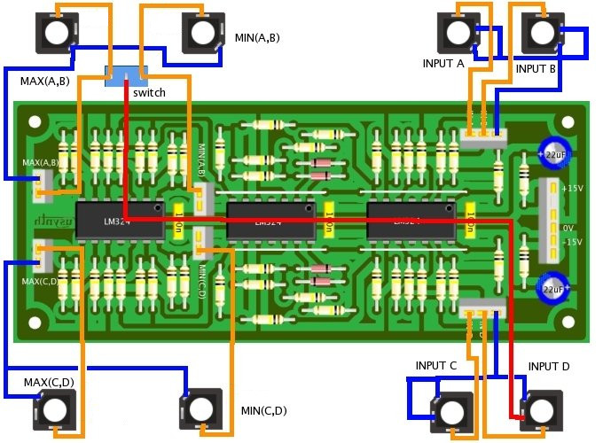
| Wiring | |||||||||||||||||||||||||||
 |
|
|
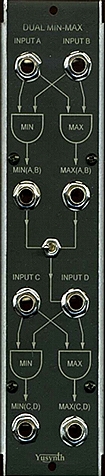
| Front panel |
||
|
|
|
Settings and trimming
|
| This circuit requires
no trimming, it must work as is. |
|
|
References |
| J. Castillo, J.L. Pérez, Instrumentation and Development, Vol 3 Nr 9, 1998:43-55  |
|
|||
|
|

