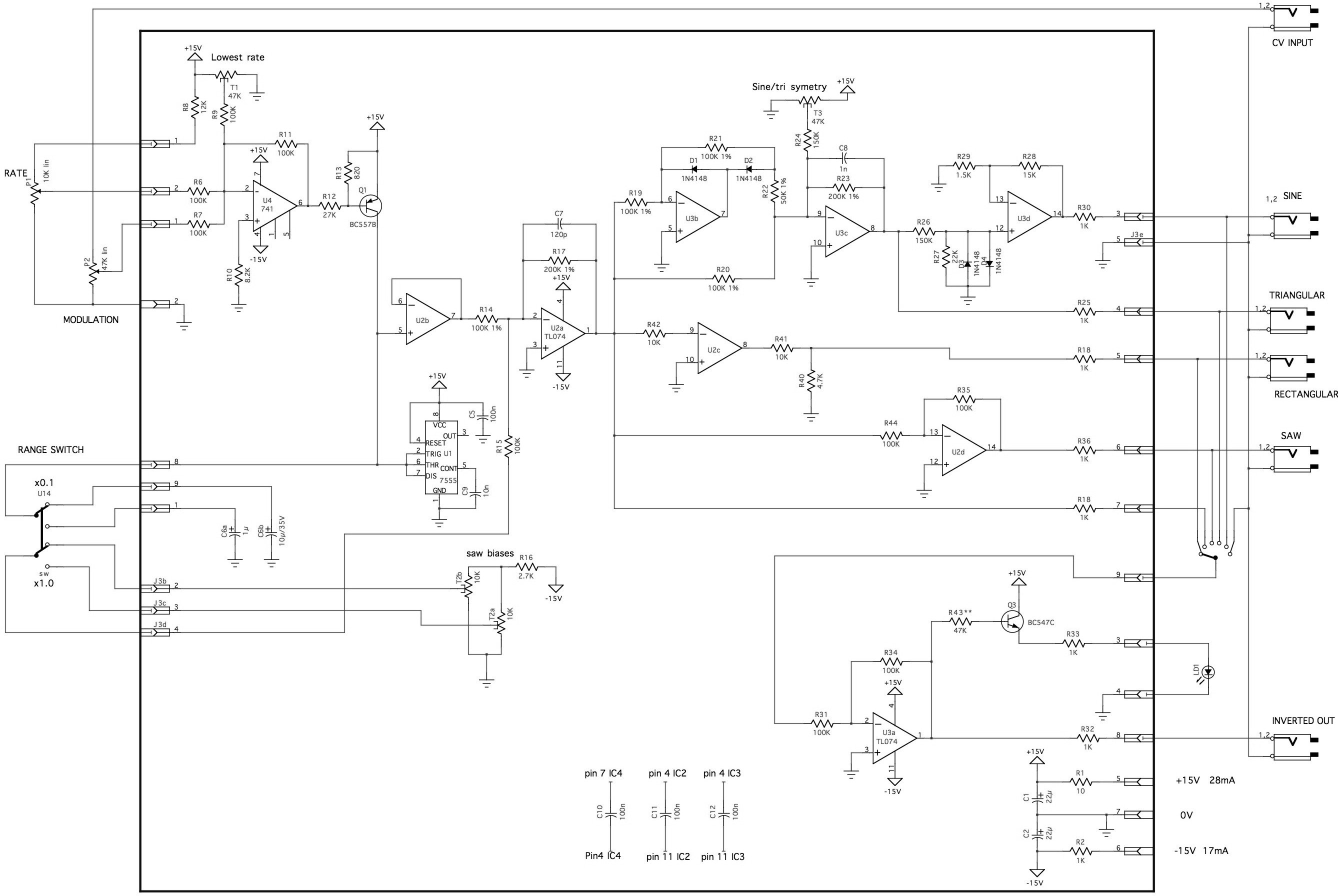
Update : feb. 5, 2009

Voltage controlled low frequency oscillator

(version #1)
En français
back to summary


Description

This module is a very useful utilty module in a modular synthesizer. It provides low frequency signals with different waveshapes that can be used to modulate and control many other modules. Another interesting feature of such a module is that its oscillation rate can be controlled by a CV.
In this version, the frequency can be set with the RATE knob between 0.1Hz (10s repetition rate) and 100Hz (0.01s repetition rate) or between 0.01Hz (100s rate) and 10 Hz, depending on the rate switch.
The frequency can be modulated in an exponential manner using the FM socket, the FM level knob let us control the amount of modulation.

The signals that are available at their own direct output sockets : SAWTOOTH (rising ramp), TRIANGLE, SINE and SQUARE.
Furthermore, the INV OUT socket provides any of the above  but  inverted with reference to the direct outputs. The signal is selected through a 6 position rotary switch : OFF (no signal), SINE, TRIANGLE, SAWTOOTH (rising ramp), RAMP (falling ramp) and SQUARE.

The oscillating heart of the circuit is based on the "design idea" by J. Brice (1976) . The wavshaper part is based on very basic classical buiilding blocks such as summers, inverters, full-wave rectifier and non-linear waveshaper.

The oscillation rate is indicated by a yellow LED, the brightness of which being linked to the signal at the INV OUT socket.

August 16th, 2006, I introduced an enhanced version, as a matter of fact when switching from one timing cap to another, the SAW BIAS setting would change. In order to have perfect waveshapes for both range I modified the schematic and PCB to add a second T2 trimmer (T2b) that let us adjust the waveshapes for both ranges.

Schematic diagram


Printed circuit board and component layout

PCB


Component layout


Download the schematic as a PDF file

Download the PCB as a PDF file

BEWARE! The document orientation is set such that it can be printed directly on "Press & peel" paper or on a mylar. In the last case, make sure that the side of the mylar with the toner lays on the copper side of the PCB.


Building instructions

reference
value
quantity
U1
7555 (CMOS version of the 555)
1
U2,U3
TL074
2
U4
LM741 or TL071
1
Q1
BC557B
1
Q3
BC547
2
D1,D2,D3*,D4*
1N4148 , * matched for better performance
4
R37,R38
10 5% 2
R33
220 5%
1
R7
820 5% 1
R14,R18,R25,R30,R32,R34
1K 5% 6
R29
1.5K 5% 1
R8
2.7K 5% 1
R17
4.7K5% 1
R4
8.2K 5%
1
R15,R16,R39
10K 5% 3
R40
12K
1
R28
15K 5% 1
R27
22K 5% 1
R6
27K 5% 1
R43***
47K 5% * off board
1
R22
50K 1%
1
R1,R2,R3,R5,R10,R12,R13,R31,R35,R36
100K 5%
10
R9,R19,R20,R21
100K 1%
4
R24,R26
150K 5%
2
R11,R23
200K 1%
2
C5
47pF
1
C2
10nF 1
C7,C8,C9,C10
100nF
4
C1a
1µF polyester film 1
C1b
10µF 35V tantalum 1
C3,C4
22µF 35V
2
T2a,T2b
10K 10 turns
1
T1,T3
47K 10 turns
2
P1
10K lin
2
P2
47K lin
1
LD1
yellow LED
1
SW1
DPDT switch
1
SW2
rotary switch 6 pos. 1
JK1..JK6
jack socket
6
C1a and C1b, T2a and T2b are switched by the range switch
Wiring


Front panel
Panel design


Download the silkscreen mask as a PDF file

Download the silkscreen mask as a JPEG file

Settings and trimming


  1. Set the FM. MOD. pot to minimum (CCW) and set the RATE pot to maximum (CW)
  2. Set the range switch to x1 (should select C1a 1µF and T2a)
  3. Connect an oscilloscope to the SAWTOOTH output
  4. Check that you have a good linear ramp with an amplitude of 10V, if the ramp is not perfectly linear, check that C1a is not leaking (be sure to use a tantalum cap here!)
  5. Now adjust T2a such as to obtain a linear ramp ranging from -5V to +5V
  6. Connect the oscilloscope to the TRIANGLE ouput
  7. Adjust T2a in order to obtain the best symetrical triangle shape
  8. Then adjust T3 in order to obtain a triangle ranging from -5V to +5V
  9. Connect the oscilloscope to the SINEWAVE output
  10. Adjust T3 in order to obtain the best sinewave shape
  11. Toggle the range switch to x0.1 (should select C1b 10µF and T2b)
  12. Connect the oscilloscope to the TRIANGLE output
  13. Adjust T2b in order to obtain the best symetrical triangle shape
  14. Set the range switch to x1
  15. Turn the RATE pot to minimum (CCW)
  16. Adjust T1 in order to obtain a RATE of 10s (frequency 0.1Hz)
  17. Turn the RATE pot to maximum (CW)
  18. Connect the oscilloscope to the INV OUTPUT
  19. Turn the rotary switch and check that you obtain the right waveforms

References


Wireless Word june 1976, J. L. Brice, Voltage-controlled ramp generator


back to summary