|
The
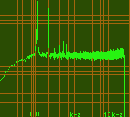
noise generator of my board tends to be contaminated
by some 100Hz hum. As a matter of fact this hum is hardly earable when
listening to the raw white noise signal but becomes more perceptible as
soon as the noise signal is injected in a VCF. When checking the spectrum
of the noise signal with a software spectrum analyzer, one can see that
100Hz, 200Hz, 300Hz, 400Hz and 500Hz overtones are superimposed to the
rather flat spectrum of white noise. These overtones correspond to
residual
ripples from the +12V rail. Because the noise generator uses a very
high
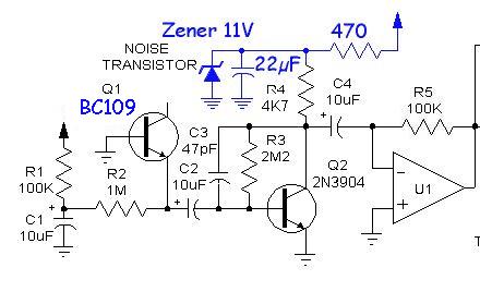
gain stage (Q2) these residual ripples are strongly amplified. In order
to cancel this overtones, it is necessary to insert a filter in the
power
supply line of Q2. This is done by inserting between the 12V power rail
and R4, a 330 or 470 ohm resistor, a 22 µF cap and a 11V
zener diode
as shown in the modified schematic diagram. The
voltage
drop introduced by this mod is quite small and the overtone rejection
is
optimal.
For
the so called pink noise (as a matter of fact pink noise correspond to
a 3dB/octave low-pass slope and actually the filter is a 6dB/octave
low-pass that gives rise to "red" noise !) be sure to use a 2.2nF value
for C5 as stated in the B.O.M. and not to use the 22nF appearing on the
schemo ! Also I found useful to decrease the value of R6 to 15k instead
of 68k. This provides a greater voltage swing more comparable to that
of the white noise. These pictures show the mods of
the PCB.
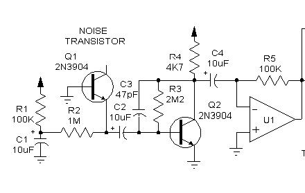
original schematic
|
modified schematic
|
|
The following images show the spectra of
the white
noise generator of the original design and of the modified design
respectively.
To view these spectra in detail click on the following reduced views.
Theses
spectra were obtained using the audio input of an Apple Wallstreet
Powerbook
G3 and the MacCRO
shareware providing for oscilloscope and spectrum analyzer functions.
The
frequency and intensity axes are in logarithmic scale. The frequency
range
is 10 Hz to 22 kHz.
|
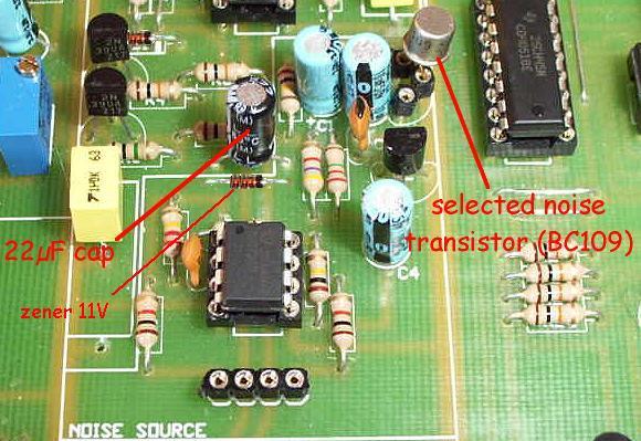
The
following images show the modifications made to the PCB tracks
and the component layout. Click on the images to get an enlarged view.
You can notice on the layout that Q1 is plugged rather than soldered.
This makes it handy to test various transistor in order to select the
nosiest ! Once found, just cut off the collector pin, otherwise it may
act as a good antenna with which you would pick the strongest local
radio station!
|
|